P/N Junctions & Band Gaps
P/N Junctions
A p/n junction is formed when two types of semiconductors, n-type (excess electrons) and p-type (excess holes), come into contact. The term p/n junction refers to the joint interface and the immediate surrounding area of the two semiconductors. If the joint is made by two separate semiconductor crystals, this is a rough interface known as a grain boundary. A grain boundary has different electrical properties than a single crystalline interface. P/N junctions are normally created in a single crystal of semiconductor by doping each side with different "dopants". The discovery of the p/n junction is usually attributed to American physicist Russell Ohl of Bell Laboratories.
The p/n junction possesses some interesting
properties. A p-doped semiconductor (i.e. boron doped silicon) is relatively
conductive. The same is true of an n-doped semiconductor (phosphorous doped
silicon), but the junction between them is a non-conductor. This non-conducting
layer, called the space charge region (see figure below), occurs because the
electrons and holes in n-type and p-type silicon diffuse into the other type of
material (i.e. electrons in p-type and holes in n-type) and eliminate each
other's charge. In a p/n junction, an equilibrium condition is reached in which
a voltage difference is formed across the junction. This voltage difference is
called the "built-in electric field", or "built-in
voltage". Electrons near the p/n interface tend to diffuse into the p-
region. As electrons diffuse, they leave positively charged holes in the n-
region. Similarly, holes near the p/n interface begin to diffuse into the
n-type region leaving fixed electrons with a negative charge. The regions near
the p/n interfaces lose their neutrality and become charged, forming the space
charge region, or p/n junction.

In the figure above, the electric field (E) created by the space charge region opposes the diffusing process (Q). There are two concurrent phenomena: the diffusing process that tends to generate more space charge, and the electric field generated by the space charge that tends to counteract the diffusing process. The carrier concentration profile at equilibrium is shown with blue and red lines. Note the two counter balancing phenomena, the space charge V-voltage and the E-field, that combined establish equilibrium.
Note that the positive and negative charges
are equal (Q graph). Also, the electric fields (E graph) neutralize each other
over the length of the junction. The space charge region has the same amount of
charge on both sides of the p/n interface, thus it extends farther from the
interface on the less doped side (the n side in the figure above). While the
charges are neutralized, the built-in voltage (V graph) is created which is
approximately 0.6 to 0.7 volts. This voltage is the significant factor in the
operation of the p/n juction and the solar cell. The voltage is like a high
wall as seen by the free negative electrons seeking positive holes forcing them
to travel through the external circuit to get to the positive holes on the
other side of the wall. The voltage provides the driving force to the electron
flow (current) created by sunlight photons striking the semiconductor and
freeing up electrons to do "work". See the Band Gap section below for
an explanation of how photon energy frees electrons from their "home
atoms".

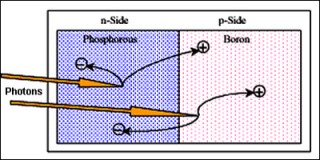
Due to the p/n junction, a built-in electric field is always present across the solar cell. When photons hit the solar cell, free electrons attempt to unite with holes in the p-type layer. However, the electric field, a one-way down-hill road superimposed across the cell, allows the electrons to flow only in one direction. If an external conductive path is provided, electrons will flow through that path to unite with holes on the other side of the junction. The above animation from Southampton University in the UK.
Effect of Temperature on a Solar P/N Junction
When crystalline silicon solar cells heat up (as on a hot summer day), all the atoms (including their electrons) vibrate faster and therefore the ability of the "built-in voltage" to separate the electrons and holes is reduced. The random kinetic energy due to the heat becomes a significant factor governing the motion of the electrons and holes.
The solar cell temperature will normally be higher than the air temperature because the panels are black and sitting in the sun. A Normal Operating Cell Temperature (NOCT) is defined as the cell temperature when the ambient temperature is 20º Celsius and the sun's insolation (captured radiation) is 800 watts per square meter. NOTCs are usually in the range of 42ºC to 46ºC.
In an experiment done by Renewable Energy UK, silicon solar panels showed a small loss of 3% power from 25ºC (77ºF) to 42ºC (108ºF). However, from 42ºC (108ºF) to 75ºC (167ºF) the drop-in power was 37% which is 1.1% per degree Celsius. In terms of efficiency the typical loss is about 0.1% per degree Celsius rise in panel temperature. For example, a crystalline solar panel that is 16% efficient at 25ºC (77ºF) will be about 11% efficient at 75ºC (167ºF).
Band Gap Definition
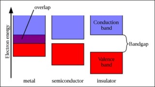
 In metals, semiconductors and insulators
electrons are restricted by atomic forces to just a few bands of energy, and
cannot permanently reside in other regions. The term "band gap" refers
to the energy difference between the top of the valence (outer electron) band
and the bottom of the conduction (free electron flow) band. In the valence band
electrons are tightly held in their orbits by the nuclear forces of a single
atom. In the conduction band, electrons have enough energy to move around
freely and are not tied to any one atom. A material with a large almost
insurmountable band gap, greater than 3 electron volts (see definitions below)
is called an insulator. In metal conductors, the valence and conduction bands
overlap, so they do not have a band gap. Materials with a small band gap, which
behave as insulators at absolute zero, but allow excitation of electrons into
their conduction bands (at temperatures below their melting point) are called
semiconductors.
 Electrons are able to jump from one band to another given an
"energy lift" by some external force, such as a sunlight photon. In
order for an electron to make the leap from the valence band to the conduction
band, it requires a boost of "band gap" energy. Electrons can gain
enough energy to jump to the conduction band by absorbing either a
"phonon" (heat) or a "photon" (light) with at least band
gap energy. Photons with energy less than the band gap will not separate
electron pairs and simply pass through the solar cell. Photons, with more
energy than necessary to separate an electron pair, do generate an electron and
a hole with the balance of their energy being dissipated in the form of heat.
Band gap energy differs from one material to another. In a semiconductor
crystal, the band gap does not vary owing to the constant energy levels in a
continuous crystalline structure (such as silicon). The band gaps in the table
below are in electron volts (eV) measured at a standard temperature of 300
degrees Kelvin (81°F).
Band Gaps of Different Materials
Definition - Electron Volt
Material
Symbol
Band Gap (eV)
Silicon
Si
1.11
Cadmium telluride
CdTe
1.49
Cadmium selenide
CdSe
1.73
Copper oxide
CuO
1.20
Gallium arsenide
GaAs
1.43
Indium phosphide
InP
1.35
Selenium
Se
1.74
An electron volt is equal to the amount of energy gained by a single unbound electron when it accelerates through an electric field difference of one volt in a vacuum. An electron volt (eV) is equal to 1.602×10⁻¹⁹ Joules which is arrived at by multiplying one volt by the charge of one electron which is 1.602×10⁻¹⁹ Coulombs. Also, by definition, the temperature of a substance at absolute zero is zero Kelvin (0 K) which is -273°C. Therefore, 300K is 27°C or 81°F.
Ideal Solar Band Gaps
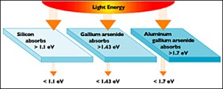
 Crystalline silicon, the most popular solar
cell semiconductor, has a bandgap of 1.1 electron volts (eV). The semiconductor
chosen for a solar cell has to absorb as much of the solar spectrum as
possible, therefore a low band gap is desirable. However, this is counter
balanced by the desire to also have as large a built-in voltage as possible
which requires a larger band gap. Therefore, as a compromise, a band gap
between 1.0 and 1.7 eV makes an effective solar semiconductor. In this range,
electrons can be freed without creating too much heat.
The photon energy of light varies according to the different wavelengths of light. The entire spectrum of sunlight, from infrared to ultraviolet, covers a range of about 0.5 eV to about 2.9 eV. The primary reason why solar cells are not 100% efficient is because semiconductors do not respond to the entire spectrum of sunlight. Photons with energy less than silicon's bandgap pass through the cell and are not absorbed, which wastes about 18% of incoming energy. The energy content of photons above the bandgap will be wasted surplus re-emitted as heat or light. This accounts for an additional loss of about 49%. Thus about 67% of energy from the original sunlight is lost, or only 33% is usable for electricity in an ideal solar cell. In a solar cell, photons are absorbed mainly in the p-layer. So, it's very important to "tune" this layer to the properties of incoming photons to absorb as many as possible and therefore to free up as many electrons as possible.
Post a Comment:
You may also like:

